
Semiconductor and PCB Test Solution
JTAG Boundary Scan Test Solution
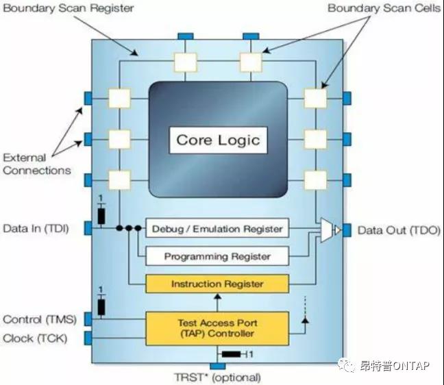
The JTAG Boundary Scan Test Solution is based on Boundary Scan Test (BST) technology. Through IEEE 1149.x standard interfaces and dedicated test algorithms, it enables high-coverage testing for PCB interconnects, BGA devices, FPGA, DDR, Flash and peripheral circuits. The solution can run independently or be integrated with ICT, FCT or automated test platforms, forming a complete production test capability with fixtures, interface boards, instruments, software and traceability systems. onTAP can provide manual, semi-automatic, fully automatic and SDK-enabled solutions based on product architecture, coverage goals, budget and automation requirements.
Customer Challenges
- Conventional functional testing is limited by firmware, interface availability and test-flow constraints, making full coverage of PCB interconnects and internal device logic difficult.
- Some communication protocols or private interfaces are not open due to IP protection, limiting traditional FCT coverage.
- As PCB size decreases and BGA/high-density devices increase, it becomes difficult to place enough physical test points.
- Large-scale logic and memory devices such as FPGA, DDR and Flash require deeper chip-level test coverage.
- ICT/FCT test systems need to work together with boundary scan capabilities instead of creating isolated equipment and duplicated fixtures.
Solution Approach
- Control the PCB under test through the standard JTAG interface and execute board-level interconnect, device pin and logic-link tests.
- Design boundary scan strategies and coverage targets based on IEEE 1149.x standards, device BSDL models and product netlists.
- Use dedicated interfaces and proprietary logic algorithms to bypass private protocol limitations and improve coverage beyond conventional FCT.
- Reduce dependence on physical test points through chip-level scan testing, especially for BGA, high-density boards and space-constrained PCBs.
- Design scan algorithms for FPGA, DDR, Flash and other devices, while using peripheral test circuits to cover ADC, optocoupler isolation and related circuits.
- Integrate boundary scan with ICT/FCT, automated fixtures, test software and traceability platforms for unified workflows and reports.
Core Capabilities
Deliverables
- Boundary scan test plan and coverage analysis
- JTAG interface, interface board, fixture and harness design
- BSDL, netlist and test vector configuration
- Test algorithm development for FPGA, DDR, Flash and peripheral circuits
- ICT/FCT integration interface, automation workflow and report templates
- Manual, semi-automatic or fully automatic test system delivery
- SDK-enabled solution selection and integration service
Business Value
- Improves test coverage for PCB interconnects, BGA devices and complex digital logic.
- Reduces dependence on physical test points and supports high-density, miniaturized and test-point-constrained PCB designs.
- Complements ICT/FCT limitations around firmware, private protocols and internal device logic coverage.
- Supports standalone operation or integration with existing ICT/FCT systems to reduce production deployment cost.
- Builds a maintainable and traceable production test platform through software, hardware, fixture and automation integration.
Specifications
- Core Technology
- JTAG, Boundary Scan Test and IEEE 1149.x
- Applicable Products
- High-density PCBs, BGA boards, FPGA boards, DDR/Flash-related circuits and test-point-constrained boards
- Integration Method
- Standalone boundary scan system or integrated operation with ICT/FCT, ATE and automated stations
- Delivery Form
- Manual, semi-automatic, fully automatic and SDK-enabled solutions
Need to improve PCB test coverage?
onTAP can combine JTAG boundary scan, ICT/FCT, fixtures, interface boards and automated test software to deliver complete test solutions for high-density PCBs, BGA, FPGA, DDR and complex boards.
Contact onTAP